Monday, June 3, 2013

AMD's 5Ghz "next generation" FX models under way!


Ok guys, finally some computex news (still not official by AMD though). Thanks goes to Hexus' and overclocknet's CPU forums .
It's semi-official, there will be a "high-TDP" FX models presented soon, gigabyte lists it as 5Ghz AMD FX lol
Original source is donanimhaber.


Some rough perf. and power estimates :
I've just read sweclocker's review of 4770K/4670K. I wanted to see what kind of difference, power wise, are we looking at Vs 8350. It turns out that in OCCT 4770K draws 140W vs 210W for 8350, both at stock. When OCed to 4.4Ghz, the power draw of 4770K spikes to 190W while performance increases roughly by ~11% or so (logical since the chip almost always tries to run at full turbo of 3.9Ghz).

Now when we look at the rumored OCed-out-of-the-box FX models, we see them having the rather high TDP of 220W. This is 95W higher than official TDP spec for 8350 (or a bit less than that considering 8350 can actually go above 125W). Now looking at sweclocker's link I posted above, the FX9000 @ 5Ghz should be sitting at 210+95~=305W. This is with 20% clock (performance) increase since both rumored stock and Turbo clock are ~20% higher than on 8350. 305W of "stock" FX9000 vs 190W of OCed to rather expected/normal 4.4Ghz for 4770K on air- that's 115W of difference, roughly of course. Since the jump with FX9000 is 20% vs the perf. increase of 10% the OC of 4700K nets, we have the FX9000 actually closing the gap when compared to OCed 4770K. Versus stock 4770K, new "stock" FX should be winning some of the benchmarks and closing the gap significantly in others. In some situations the gap will still be there though and with a hefty power difference at that.

Finally the pricing structure. If AMD prices these parts at lower range than 4770K, somewhere close to 4670K or a bit higher (250-260$), it could be an "OK" purchase for those wanting great MTed performance and somewhat competitive ST performance (5Ghz Vishera is pretty fast chip in ST tasks, still slower than IB and co though). Lastly those buyers should be ready to accept the fact their chip will be drawing >120W more than OCed IB/Haswell setup,but will be cheaper ~100$ or so.
__________________

4770K/4670K (Haswell) reviews

Haswell has launched and brought us fastest yet x86 performance. It's great to think we have come so far from 2006. Still, the performance jump from IvyBridge core is pretty disappointing in legacy code( FMA3/AVX2 is another story, yet to be written when software support arrives).

Here is a XS topic that covers most if not all reviews so far.
Enjoy.

Saturday, June 1, 2013

Kaveri is FM2 compatible?


Roy Taylor spoke for newegg TV about Richland. Interesting remark from him at around 3:23 in to the video . Kaveri will be compatible with FM2 boards according to him .We know that AMD lists Kaveri as FM2+ so my guess is that it's compatible BUT you would want FM2+ board with GDDR5 or DDR4 (whichever it supports) in order to get the best possible performance.
Sunday, May 26, 2013

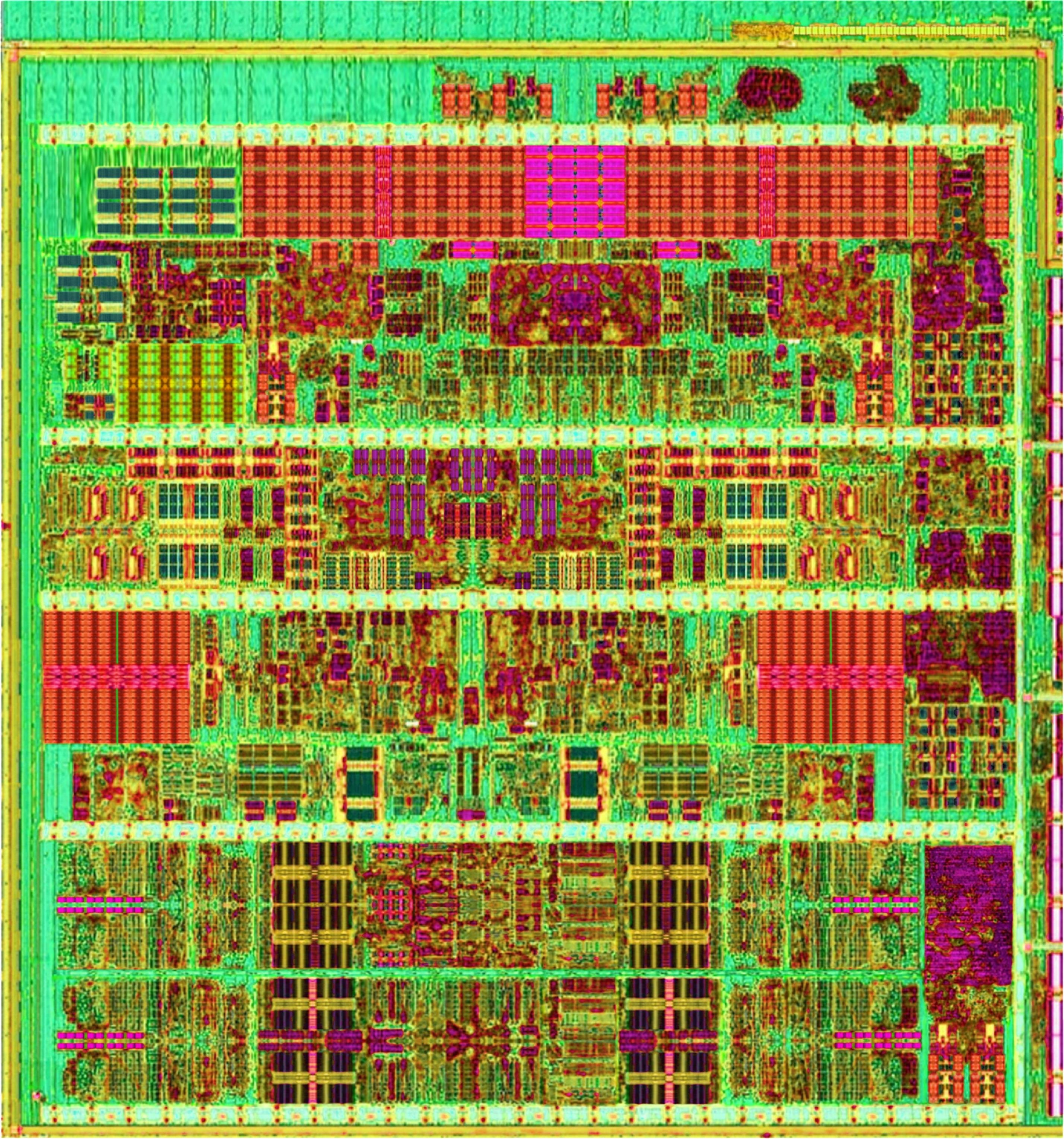
AMD Steamroller die shot leaked?

Poster Fellix_Bg posted an interesting picture on the Xtreme systems.

It looks like it could be legit die shot but anything is possible. The changes to the core are massive, especially the front end, branch prediction,instr. and data caches and FP unit as well(massively bigger dedicated die area - 2x the die area dedicated for FP in BD/PD).


Higher res. image


There is also some discussion on SA forum about it and comparison of functional units in this die shot and the BD/PD ones.
SA forum member sdlvx made a nice comparison image:

EDIT:

Two posts from knowledgeable people. 1st is Hans de Vries at SA forum:


This seems quite legit and it's a big module indeed.... It seems many resources are doubled:  
Floating point: dual 256 bit FMA instead of dual 128 bit FMA.
Integer: 8 ALU's and 8 AGU's instead of 4 both. Dual 32kB data caches instead of dual 16 kB.
Many other resources are also doubled like rename hardware and so on.


This is how I understand this design (on inf64's request):

The single Bulldozer decoder somehow couldn't handle 2 threads running
at 100% and for benchmarks we see at most a 50% performance increase
when the "second core" becomes active. So it doesn't work good enough
for CMT (but it's more than OK for dual threaded SMT)

Now why not double up the decoder and use the capability to decode
2 threads for SMT instead?

The dual 6 cycle 256 bit FMA FP units "cry out loud" for more threads,
they will be idle and unused otherwise for most of the cycles since you
need 2x6=12 FP operations to go on simultaneously to fully utilize them.
Even with 4 threads that's still 3 FP operations in parallel per thread.

The old 128 bit FMA units used the hardware more efficiently with two
cycles used per AVX operations but I guess one needs full 256 bit AVX
units to score well at these specially designed synthetic, but otherwise
pretty useless, benchmarks.

A single "Integer core" now has 4 ALU's and 4 AGU's which can improve
the integer performance somewhat, but not a lot. Actually I hope they
can still function as dual 2 ALU/AGU integer execution cores to support
4 threads in parallel. That would really help multithreaded performance,
and a little bit of the CMT ideas would survive.

Over time, in subsequent versions, they can now incrementally improve
single threaded performance using 4 ALU as much as possible. But even
then. Integer performance wasn't really Bulldozers problem as can be
seen in the Boinc Dhrystone benchmarks which showed a similar integer
IPC as the Athlon/Phenom cores (as long as the benchmark fits in L1D)

The L1D caches are doubled to 32kB to support 256 bit reads and writes.
A single cache line of 512 bit can now be read and written in a single
cycle freeing up cycles for more program reads and writes. The double
width also reduces bank conflicts.

This strategy to improve Bulldozer/Piledriver is pretty much as I would
have done it. I hope it's indeed AMD's way as well.


Hans.


Second is from 3dilettante B3D forum:
 For fun, I'll just assume this is a true representation of a future core, or someone put a decent amount of effort into making this up.
There isn't a good shot of this core and Bulldozer of equivalent quality, but here's what it sort of looks like to me.

The L1 has two sections, separated by a pink section that could be the microcode ROM. There is what appears to be a fetch buffer for both sections, so I am left wondering if this is one big L1 I$ or two.
For the instruction section there are two of everything, save the predecoder, branch predictor, and microcode. It think there's a little pink rectangle below the microcode that is a microcode-related engine, and even this is duplicated.

A single integer core looks to have twice the integer ALUs, twice the AGUs, but the multiplier and divider sections don't look replicated. The physical register file doesn't appear to be doubled. If it is bigger, it's not significant enough to split it into new sections or appear to be more than incremental growth.
The portions of the pipeline related to gathering operands and immediates for each instruction are doubled.
Interestingly, it looks like the rename tables and retire structures are doubled in size.
The table that might have to do with waking up/picking instructions could be bigger, but it isn't doubled.
The odd thing from a single-threaded perspective is that the scheduler logic outside of the tables is either much denser or not much larger. It's also not really necessary to have double the retirement tracking or rename tables for a core whose decoder is still 4-wide--if the core is single-threaded.
Perhaps it isn't.
If the integer pipeline is partitioned into halves, it might make the bypassing network less of a nightmare than expanding it from 2 ALUs and 2 AGUs to 4x4 single-cycle.

I've only had fuzzy BD shots to compare with, which makes the load/store section particularly hard to analyze.
The L1 data cache appears to be different, but not necessarily much bigger in area. If it's not bigger, it may be more aggressively banked. The interfacing logic on the side of the L1 doesn't appear to have more subunits, which might mean the port count hasn't changed. I don't know if its bandwidth has changed, but the fuzzily pictured width of that interface doesn't seem to be much different.
The L/S section appears relatively narrower compared to the sections that did grow, which could indicate it has been slightly modified.
There are a few duplicated/grown structures, which might be queues for loads and stores. My die-shot-fu isn't good enough to know which one is which. The more obviously duplicated structure may be a pair of store queues.

The FP unit appears to have rotated a bunch of components 90 degrees, and doubled the capacity of the register file. The two halves of each bank of registers aren't physically identical. This may be a legacy/full vector set distinction.
For what it's worth, what watchimpress stated is the retire control is duplicated. There were already two banks, one per thread with the original dual-threaded FPU. This could mean it's now able to support four.

I think there is still an upper/lower data path split, but I'm not sure which way is best to handle it.
The units themselves have a double pink line through the middle, which may be a way to separately gate each half.
It may be better to rotate the whole FPU 90 degrees. Instead of it being left:right=Hi:Lo, it's left=register file 0, right=register file 1.
Each half would have its own Hi:Lo split. There seems to be some extra routing going on between the upper and lower halves of each side to permit shuffling between them.
There's a slight break in the symmetry of the left and right sides, however, particularly in the lower right. There may be some special functions that use different hardware there. There is some additional routing in the lower half that could explain how one half could still use whatever special hardware is on the other side.
This may also explain the potentially narrower depiction of the FPU in some slides, which went form 2 FMAC+ 2MMX(one being also FSTORE) to 2 FMAC + 1MMX. The hardware would be mostly the same, but the common case would be that each thread can only see its side of the FPU and other ops that could cross to the other side have the one port doing double-duty.

Monday, October 29, 2012

AMD Vishera launches,finally. Bulldozer done right

1 year has passed since my last post which covered ,you guessed it,a Piledriver core. I predicted 4.2Ghz base clock (overstated by 5%) and 5% higher IPC( understated by 3% on average,it varies between 5% and 20% depending on workload). So basically I predicted 4.2Ghz Vishera and expected 20% higher performance. What we get is 4Ghz Vishera that is ~15% faster,pretty much what I said minus the higher clock ;). Also Vishera, as we will see later, outperforms Bulldozer core on the same clock in games by a very high 13.5%,a feat I didn't expect! On to the Piledriver launch details then. But first a little bit of history.

AMD promised a lot of things when it comes to long awaited Bulldozer core. On many levels they didn't deliver but on some they did. Now,one year after Bulldozer version1 ,we finally have a "quick  fixed" Enhanced Bulldozer(how AMD called it 1 year ago). Does it deliver? Yes it does. On many important levels,this core is what Bulldozer should have been when it launched. But AMD needed something last year and they went with what they have. Now finally,albeit late, the Piledriver delivers. It's faster per clock,consumes less power at the same targeted clock and does this without Resonant Clock Mesh or a smaller node. It's a tick+ in intel's terminology since what it delivers in IPC and clocking is more than what IvyBridge did with a uarchitectural tweaks and a die shrink.

Some relevant links to reviews(there are many reviews, for a complete list go to this topic @ XS where Flanker did a great summary of all the data):

http://www.planet3dnow.de/vbulletin/showthread.php?t=408737
http://www.hardware.fr/articles/880-1/amd-fx-8350-retour-amd.html
http://www.tomshardware.com/reviews/fx-8350-vishera-review,3328.html
http://www.anandtech.com/show/6396/the-vishera-review-amd-fx8350-fx8320-fx6300-and-fx4300-tested


Models summary:


Piledriver die shot:


Here are slides that detail uarchitectural improvements:

And how does it do in reality versus Bulldozer version1 you ask? Look for yourself:
Hardware.fr chart

7.7% average IPC gain in application workloads and 13.5% average IPC gain in gaming workloads. Job well done AMD! This core does work more efficiently AND clocks higher within same power envelope which results in greater power efficiency.

For comparison between 3770K,Thuban,Bulldozer and Piledriver (all @ 3.6Ghz) check planet3dnow review linked above. Piledriver comes really close to 3770K in many real life  workloads and offers great bang for the buck.

Average performance in applications:
FX8350 @ stock offers 94.4% of 3770K stock performance for 100$ less. The above is average from many workloads some of which are not multithreaded. A 15% improvement versus 8150 is very good result and is close to what I speculated 1 year ago.  FX8150 has very high full core/half core turbo of 3.9Ghz and this is why the difference is not more than 20%. If it ran closer to 3.6Ghz in most workloads(as it doesn't,it's at 3.9Ghz most of the time), the difference between 8350 and 8150 would be >20%.

Gaming performance average:

 FX8350 is considerably slower (at stock) than intel parts in selected gaming benchmark suite hardware.fr used(very CPU bound games and Skyrim is one that particularly doesn't like AMD CPUs for some reason so the average is dragged down quite a bit). Still FX8350 does very nicely compared to all other AMD CPUs and now has a respectable score ,basically on par with 3240 i3 and some 15% lower than Quad core Ivy Bridge 3330. This is more than enough level of performance for modern games and unless one plays exclusively those few titles that run bad on AMD hardware(like SC2 or Skyrim), FX8350 will be a great budget gaming processor. Once OCed to ~4.6Ghz which is common for 8350/8320, this chip would be ~18% slower than what 3770K offers in games hardware.fr used,for 100$ less.

In summary of this short post, FX8350 is what AMD promised: a better Bulldozer in every way you can think of. It has considerably higher IPC ( for a tick or a "quick fix"), it clocks higher and does it within same power budget on the same (bad) 32nm GloFo process node. Let's hope AMD brings SR core to FX line and doesn't abandon this market segment like some rumors are suggesting. Even with Haswell on the 2013 horizon I believe Steamroller has a chance of coming ever closer to intel desktop lineup since it massively improves single thread execution ,an area in which AMD still lags intel by a quite a margin. Multithread performance is good now and is very competitive. The last "bad" thing about BD/PD is power draw and this won't be fixed until 28nm node is ready. For those who don't mind about higher power draw (most don't since PC idles 95% the time anyway and difference is zero there), the FX8xxx line is the perfect choice for a mainstream PC desktop user on a budget.


Wednesday, October 26, 2011

What comes after FX? FX Next

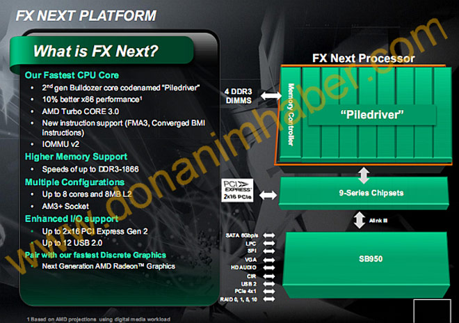
After not so successful launch of their new flagship desktop processor,AMD started talking up their next chip that will succeed Bulldozer Ver1. Say hello to FX Next ,based on Piledriver core :


Piledriver is supposed to fix certain shortcomings in BDver1 processors. I summed up some of them in my previous blog so I won't reiterate those.
What will AMD have to offer before Piledriver arrives? The following roadmap gives us some clues:

FX8170 is supposedly launching in Q1 2012. It will be based on new (somewhat improved) B3 stepping. Hopefully B3 will be enough to polish speed path issues (if there are any) and bring up clock speed. The rumored 8170 is supposed to run at 3.9/4.2/4.5Ghz clocks. This is a very solid uplift(~7.7% over 8150). Bad news is that there is no "8190" on the current roadmaps and 8170 is supposed to tide AMD over until PD arrives in Q3. That is 2 quarters... Good news is that PD will be overall 10-15% faster than what AMD has at the moment of its introduction (so 8170). This lines up well with rumored ~5% IPC increase over BD with the rest being clock speed.
So:
Q1-Q2 2012: 3.9/4.2/4.5Ghz FX8170
Q3-onward : 4.2?/4.5?/4.8?Ghz FX8280?
Effectively 4.2/3.9=1.07 or 7% clock uplift with PD. Now count in the IPC uplift of 5% or so : 1.07x1.05=1.12 or 12% overall faster than 8170. AMD said 10-15% more x86 performance with PD so this slides right in the middle of this projected figure. How much is this faster than current 8150? 8170 should be around 7% faster than 8150 so 4.2Ghz(base) PD based FX is going to be roughly 20% or so faster than 8150. Not a bad upgrade if you look at it from time perspective : 8 months after BDver1 we will get 20% faster FX part (stock vs stock). It's not unreasonable to expect better OC and thermal characteristics too,so all in all it will be a good "fix" for current BD desktop competitive situation.

PS All info above is my interpretation of available data. I used "best case scenario" above. Real PD core and 8170 may turn out to be totally different than what I speculated. We have seen this happen with BD core. Since back then I also based my predictions on publicly available data coming from AMD(which turned out to be a bit optimistic on their side) , this may happen again with PD and 8170. So take it as it is,just speculation.

Thursday, October 13, 2011

Zambezi : 2nd look.

OK, I have read a lot of reviews now. Some things are clearer now.
I suppose I overreacted a bit in my previous blog. Zambezi is hot ,but overall it's not a slow chip. It performs rather well in MT applications. It does have some weaknesses which AMD must correct. Some of the weaknesses are not solely AMD's fault,but GloFo's too.

So this is what ,in my humble opinion , AMD must focus on in the future ( think Piledriver and Steamroller):
1) First and foremost AMD must invest heavily in relationship with developers. They must hire a brand new team of both young and motivated guys who will literary go out and help developers in order to maximize the potential of Bulldozer design. This first iteration is just that ,first. It has some flaws which AMD will try to fix and hopefully succeed in that task. But underlying design ,which is truly revolutionary , will need GOOD software support in order to give best performance to the end users. This means FMA4,XOP,BMI and the rest will need to be properly supported in future multimedia desktop workloads. Notice I'm speaking about DESKTOP space here. Server is in no such need since recompiling is a norm there.

2) AMD must improve the cache performance,especially L1 and L2 writes. This is a major bottleneck and it shows its ugly face in many workloads. AMD is aware of this and hopefuly Piledriver has at least somewhat better write performance with these two levels of cache. L3 looks fine,even more than that. It is much faster than L3 on Thuban.
They also need to work on improving the FP unit. It may be great in FMA4 stuff but it's much less impressive in legacy SSE or AVX128 workloads. Maybe expanding it a bit and expanding the buffers could help. Single thread performance is not anywhere near what this thing SHOULD be capable of so there must be a bottleneck somewhere since in numerous SIMD workloads it's not faster than K10's single core(and its 128b unit).

3) AMD must twist GloFo's arm very hard and very fast. Not only their 32nm production is bringing many defective Llano parts (which is truly a shame since most of the time GPU is broken and then it's not APU any more), but now they can't brake 3.6Ghz barrier on a design that was SPECIFICALLY DESIGNED FOR CLOCK speed (while it does have some IPC improvements in certain areas too). So original goal set by AMD was 30% clock uplift with the same power draw as previous design. We get this ONLY in limited Turbo mode now. We should have 4.1Ghz 125W stock clocked Zambezi parts with 4.7Ghz half core turbo and 4.5Ghz full core turbo. This Zambezi would effectively be 12% faster than 8150 with same power draw. This Zamebezi would allow AMD to use SMT core affinity scheme and release a patch for windows 7 that would force threads first to modules and not cores. Performance uplift is ranging from 5% to massive 40% in some cases,averaging to around 15-20%,depending on benchmark selection. 

So what we need is 95W 3.6Ghz FX8150, 125W 4Ghz 8170 and 4-4.2 Ghz 125W 8270 (Piledriver).
This lineup would hold off  SB and IB ,at least in mid and mid-high performance segments,without many problems.

4) AMD should work closely with MS and release a patch to windows scheduler. As in link I've provided above, performance uplift is not a small number but a very nice 15-20%.
 Trade-off is power draw though. All is explained well in this great review by harware.fr .

So there you have it. Bulldozer is not what we expected,but it's not a complete failure either. It's a solid chip which will shine in future applications ,which are going for multiple threads. Single core speed ,while still important,is not the main selling point any more. For those who want a good single core performance while having great MT performance (but still slower MT performance than FX8150) ,they can pick 2500K . It's the best chip by intel currently from perf./$ POV. 8150 is not as good but very close! It needs 10% shave from it's MSRP and AMD may sell a sh*t load of these things :).